900MHz Cordless Phone Bugging.
The purpose of this project is to explain how a cordless phone works.
You are allowed to build this project, but the law forbids you to use it
in the purpose to listen to other peoples phone conversations.
I tell you this because I don't want to be sued (*smiling*).
All contribution to this page are most welcome!
Background
In the old day the cordless phones were working at 45MHz.
Today they have moved up to 900MHz. It is not easy to build stuff for 900MHz so in this project
I will re-use an old cordless 900MHz phone I found in a container.
Since you wont have the same phone as I have, you might think this is not a project for you, Wrong!
Read this and you will learn how do identify parts in cordless phones and you can rebuild almost
any model.
Remember we are now still dealing with analogue signal. The digital phones are a bit different.
In the future I will present a decoder for the digital phones as well.
If you have any knowledge about this subject, do take contact with me, I need help.
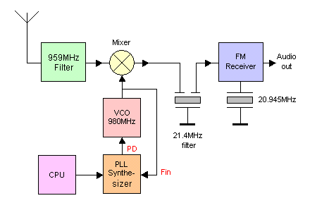
Block diagram
This is a block diagram of an analogue 900MHz cordless phone.
I will show you only the receiver part. The transmitter part is not interesting because we don't
want to transmit anything.
The RF signal is first filtered and amplified in a 959 MHz filter.
The RF signal will then enter a mixer to be down converted to lower frequency.
To the mixer you will find a VCO (Voltage Controlled Oscillator). The frequency from the VCO
is controlled by a PLL synthesizer. The PLL synthesizer probes the VCO frequency (Fin),
and adjust the "PD" voltage until it finds and locks to the programmed frequency.
The product out of the mixer will pass a filter (21.4MHz in my case) and then enter a
standard FM receiver circuit to demodulate the sound.
Since we don't know how to program the PLL synthesizer we can not set the VCO frequency and
thereby not tune the receiver.
What should we do then?
I suggest we rip out the PLL synthesizer and replace the "PD" with a potentiometer.
Simple solution, don't you think!
The "PD" is a voltage which control the VCO and by using a potentiometer we
will be able to tune the VCO manually and receiver all signals in that band.
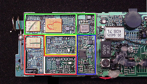
Forget about all details now and let's look inside a phone and try to identify the parts.
In my phone I found a shielded box of 4x4 cm. I removed the cover and took some
photos. To left you can see the antenna as a spiral. There is four section in my box.
The first thing we see is a black circuit in the blue frame, three yellow boxes in the
green and red frame and outside the box you will see a crystal and a black box with text "455D"
and under that some kind of tuneable coil.
I know that the cordless phones receive at 959MHz and transmit at 914MHz. If you look again in
the red and green frames you will find two yellow cubes with label 959 and in the red frame 914.
This yellow cube things is filters and preamplifier. Now we can easy understand that the red frame
is the transmitter part and the green is the receiver part. The blue frame has an ic circuit.
It is the PLL synthesizercircuit.
Finally the yellow frame is the VCO. You may think it is not this easy to identify all block,
but I will now look into each frame and I will show you details that will confirm the function
of each block.
Outside the shielded case you will se a crystal and under the crystal (you can not se it on
this pic) is a 16 pin SO IC-circuit MC3371. If I look into the datasheets I find that
this circuit is a FM receiver. The black box below the crystal with the label 455 is easy
to identify, it is a ceramic filter for 455kHz. Below that box is a tuneable coil which
must be the quad coil.
Now lets look into each block in more details:
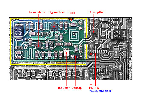
VCO:
The picture above show you the yellow frame, the VCO. I have removed the PLL circuit because
we don't need it and it hides the wires on the pcb.
A VCO is an oscillator which is voltage controlled. The oscillating components are a
coil and a capacitor. To change the frequency you need the capacitance to be voltage controlled.
This is done by a varicap. In the PIC above you will find the varicap and the coil at the bottom.
The LC circuit needs a transistor to keep it oscillating and this transistor is Q1.
If you follow the strip line of the pcb you can actually see that the coil and varicap
is connected to this transistor.
In my block diagram you can see that the PLL circuit has an output called PD which is connected
to the varicap to set the VCO voltage. If you follow the strip line of the varicap to the right
and through two resistors you end up at the PLL circuit.
The VCO signal from Q1 is not so strong and is amplified in Q2 and goes out of the yellow frame
through a hole (Fout) to the mixer (I show you later).
So what does Q3 do?
Look again at the block diagram and you will find that the PLL need to probe
the VCO to know the frequency of the VCO. A small portion of the VCO signal is amplified by Q3
and then goes to the PLL (Fin).
If we now want to control this VCO by ourselves, the only thing we need to do is to change the
voltage at PD (The VCO voltage). If we connect a frequency counter at Fin to the PLL we can
measure the VCO frequency.
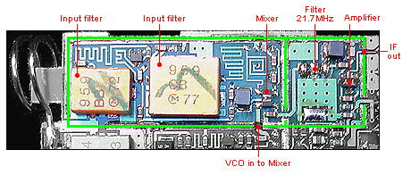
Input receiver:
The picture above shows you the green frame, the input stage of the receiver. The two yellow
cubes is 959MHz filter and if we follow the strip lines we end up at a dualgate fet. The other
input of this fet is connected to the VCO, now we understand that this dualgate fet is the mixer.
Is also has a label "M" printed on it. I don't think it stands for MacDonald...
The output signal from the mixer goes to a filter, looking like a crystal. I have removed this
filter on this picture. Anyhow you can see it in other pictures. The filter is also labelled
with 21.7 MHz. You can find this filter in the block diagram as well.
The output from the 21.7MHz filter is then connected to a transistor to amplify the signal
(IF out) before it enters the MC3371 FM receiver circuit.
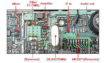
FM receiver circuit:
The picture above shows you the outside of the shielded box. You can see the mixer and 21.7MHz
filter I described above. In this pic I have lift up the crystal and removed the 16 pin
SO-IC circuit MC3371. If you look into the datasheet of this circuit you will find that the
RF input pin (IF in) is 15 and the Audio out is at pin 9.
Squelch control:
This circuit has something called squelch control. It is a unit that shut of the audio
if there is no incoming RF signal. I don't want this receiver to have any squelch control
so I disconnect it by breaking the wire at pin 14 (se datasheets).
What do we need to do to modify this phone so we can use it to receive all signal around 959MHz?
We need to remove the PLL circuit and replace the "PD" voltage with a potentiometer.
We connect a audio amplifier at the audio output of the FM receiver circuit and finally we
disconnect the squelch trigger.
That is all!
Even if you won't find this exact phone you can use this knowledge to identify your own phone.
If you have problem you can take a photo and I will help you to identify all parts.
Final word
After reading this project I hope you will have greater knowledge how to
identify the different parts in a cordless 900MHz phone. Please don't use this
project in the wrong way!
You can always mail me if there is anything unclear.
I wish you good luck with your projects and thanks for visit my page.
 900MHz Cordless Phone Bugging.