 Power amplifier class-C
Basic function
Class C is defined as an anode conduction angle of less than 180 degrees. In Class C, the amplifying device is deliberately not operated linearly. Instead, it is operated as a switch in order to reduce resistance loss. The anode conduction angle in Class C operation is usually made as short as is possible. In effect, the tank circuit makes the RF output sine wave--like a bell that is struck at a constant rate by a hammer. This is similar to the principal behind the spark transmitter.
The efficiency of a typical Class C amplifier is high. When compared to a Class AB1 or Class AB2 amplifier operating at the same power input, a Class C amplifier will deliver a received signal increase of about 1db--in other words, 1/6 of 1 S-unit. However, significant trade-offs are required to achieve that 1/6 of 1 S-unit. As is the case with Class B operation, the distortion from Class C operation is so high that SSB operation is precluded. Only CW, FM or FSK operation is practical. The harmonic output level from a Class C amplifier is substantial. Extra filtering is usually needed to control harmonic radiation.
The maximum available power in Class C operation is roughly three to four times the anode-dissipation rating of the electron tube.
To simplify, you can think of the transistor as a switch, which is on or off. The figure below show the two working states.
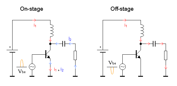
First lets have a look at the schematic. To the base of the transistor is a AC-generator connected. This signal will make the transistor conduct during the positive period. A coil is connected from power supply to the collector and there is a capacitor connected to a resistor. The capacitor at the collector remove the DC voltage and the resistor is simulating the antenna.
During the positiv period of the input signal (On stage)
During the positiv period of the input signal the transistor will conduct (On-state). You can imagin that the transistor is a switch which connects the emitter with the collector.
What will happend now is that the current I1 (red) flow through the coil and then into the transistor and down to ground. A magnetic field builds up in the coil depending on the magnitude of the current. At the same time the voltage over the capacitor discharge through the resistor making another current flow I2 (blue) also through the transistor. The I2 current passes the resistor (antenna) which radiate the energy.
During the negativ period of the input signal (Off stage)
During the negativ period of the input signal the transistor will not conduct (Off-state). You can imagin that the transistor is an open switch. No current can pass through the collector to the emitter.
The magnetic filed which was build upp in the coil will now collaps and generate a current I1 (red) which will flow through the capacitor and into the resistor (antenna).
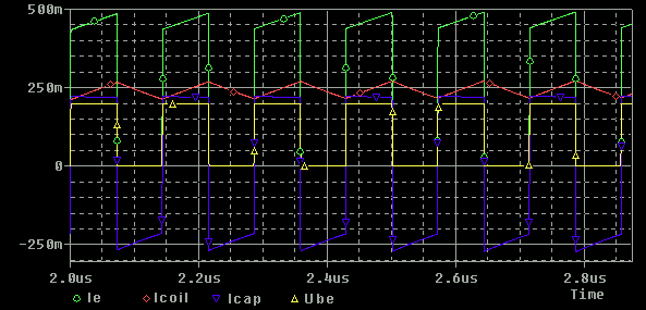
Lets take a look at a current-simulation of this circuit.
I have made a Pspice simulation of the circuit above. Since the circuit above is a simplification of a PA I hope you will oversea the square-shape and magnitude of the signals. In real life the signal will have a sine-wave shape. The important thing in this section is to understand how the current flow.
The frequency in this simulation is 50MHz, Vcc = 12V, L = 15uH, C = 10nF and the resistor is 50 ohm.
Don't get confused by sneaking at the simulation, keep reading and I will explain all shapes.
Lets start with the yellow signal. This signal is the input to the base. When this signal is high, the transistor will conduct(on-stage) and when it is low the transistor will be (off-stage).
The red signal is the current I1 through the coil. When the transistor is ON this current is increasing building up the magnetic field and when the transistor is OFF, the current decrease and the magnetic filed is collapsed.
The blue line indicate the current I2 through the capacitor and the resistor. This current is changing direction depending on the ON/OFF stage of the transistor. This current will be radiated into the antenna. Notice that the current is swinging around the zero line.
The green line indicate the total current through the emitter I1 + I2 during ON-stager. If you compare the blue current with the green you will notice that the green current is about twice the size the blue current. Another difference is that the blue current is never constant zero it is changing polarity all the time while the green current is zero half the cycle. You can think of it like this: The antenna is constanly delivering energy to the air (blue current) but the transistor is only deliver energy half the time (green current) so when the transistor deliver energy it must be so much so it cover the other half period when it sleeps. The coil is the tank where the extra enery is stored for the sleeping period.
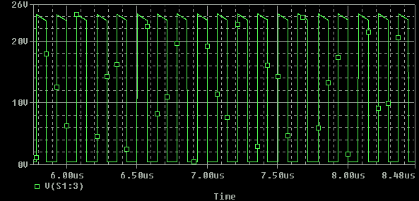
Lets take a look at a voltage-simulation of this circuit.
The green line represent the voltage at the collector. When the transistor conduct (On-period) the collector-emitter voltage is equal to the saturation voltage of the transistor (some hundred millivolt). The voltage at the collector is close to zero. When the transistor goes to the OFF-stage the coil will induce a voltage equal or greater than the power supply. Since the coil is connected to the positive power supply the induced voltage will be added to the powersupply which makes the peak-voltage at the collector to 2 * Vcc or more.
The amplitude of the signal at the collector will be equal to the Vcc (12V in this case). You will read more about this subject in the power- calculation a bit down.
One important thing to notice is that the collector-emitter voltage at the transistor swing to high levels and some transistors are sensitive for breakdown so you must make sure to choose a transistor that holds for the voltage level or else you have to decrease the voltage.
I have now given you a short introduction of the basic functions and the current flow in a power amplifier.
Next section will explain how to match the input of the power amplifier to previous drive, to get the best performance of the power amplifier.
Input filter (impedance match)
Since most most RF equipment (input/output) are matched to 50 ohm, we will try to match the input impedance of our power amplifier also to 50 ohm. The impedance from the base to emitter in the transistor is very low, 3-10 ohm depending on the transistor you are using. As you might understand, it wouldn't be a great idea to connect a RF driver made for 50 ohm to our 3-10 ohm power transmitter. The driver would probably give you a small pyrotecnical show, which could wait until new years eve.
What we want is to match the impedance in the input stage so we can drive it with 50 ohm and transform all the input energy into the transistor base-emitter which is still 3-10 ohm. There are several ways to do this. One is to use a transformer with different turns of winding or like in this construction, we will use two variable capacitor and a coil to find the best match.
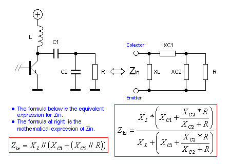
Schematic of Input stage
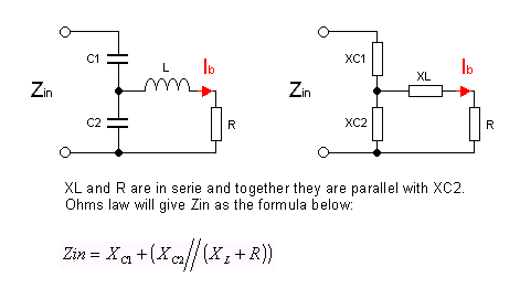
The fig above show the input stage to the transistor. Zin is the input impedance of this power amplifier. We want it to be 50 ohm so it will match the output from a previous drive stage. C1 and C2 is tunable capacitor and the resistor R in this shematic represent the input impedance of the transistor between the base and the emitter. A serie coil (L) is inserted between the base and the two capacitor. The two capacitor and the coil will transform the 50 ohm input to the 3-10 ohm impedance of the transistor and all input energy will end up in the transistor. The current Ib is the current into the base of the transistor.
What do I want to find out?
I want to know the values of C1, C2 and L so the impedance will be 50 ohm and to get maximum current Ib. To achieve this I need to find some mathematical formula. To make the calculations more simple I transform the capacitors and the inductor to reactances. You can see this in the right schematic. As you probably can see, the XL and R are in serie, and together they are in parallel with XC2.
The formula at the bottom of the figure is the expresion of the impedans Zin.
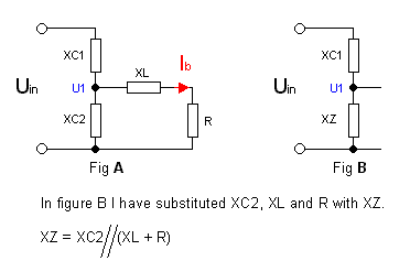
To simplify the branch with the XL and R parallel with XC2, I substitute them with an impedance called XZ.(See left fig below).
 |
 |
Puhh, I think you need a coffee break now, at least I do, then we can discuss the formula at the right pic.
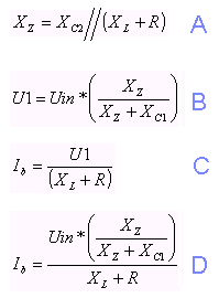
The first expression A has already be mentioned, XZ is the substituted impedance. In figure B (see fig above) you can see that after the substitution, we will have a simple voltage divider with two impedances (XC1 and XZ).
If I would apply a voltage Uin over the two impedances I could calculate the voltage U1 by using formula B.
Now when I have the epression for U1, I can then calculate the current Ib C & D, since I know the XL and R.
Summary: All formula are in complex form. (Real part and Imaginary part).
I have the expression for the total input impedance and the expression for the current Ib.
As you can see we have three components to play with C1, C2 and L. There are some ways to calculate each components, but I have not found any easy and understandable expression. If you have one please mail me and I will include it here. I solved the problem in a more practical way. Lets say I want my PA working with 50MHz and transistor impedance (R) is 10 ohm. I set Uin to 1V to make it simple during my test.
 I made a small computer program which looped and tested about 400.000 combination of different values. It is not so difficult as it might sound.
I made three loops. One for each component and I run the C1 and C2 from 1pF to 100pF and the coil from 5nH to 400nH.
For each itteration I increased the value of one of the components.
The program put the values into the formulas and stoped running when C1 and C2 was 100pF and L was 400nH.
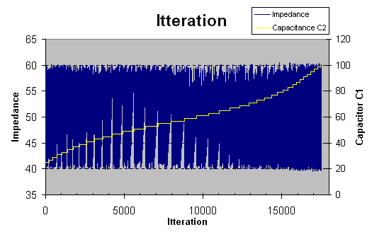
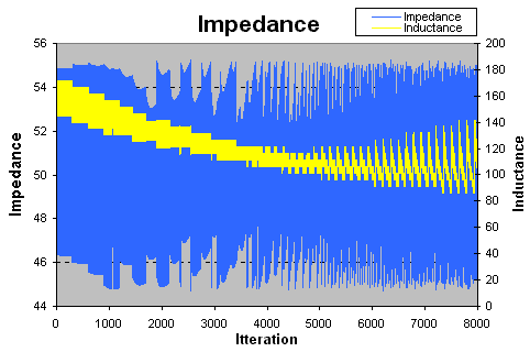
Remeber we wanted the input impedance to be 50 ohm so I saved all values which was from 40 to 60 ohm impedance. The graph bove
show 18.000 itteration which gave me the impedance of 40-60 ohm. I will now explain the graph.
I made a small computer program which looped and tested about 400.000 combination of different values. It is not so difficult as it might sound.
I made three loops. One for each component and I run the C1 and C2 from 1pF to 100pF and the coil from 5nH to 400nH.
For each itteration I increased the value of one of the components.
The program put the values into the formulas and stoped running when C1 and C2 was 100pF and L was 400nH.
Remeber we wanted the input impedance to be 50 ohm so I saved all values which was from 40 to 60 ohm impedance. The graph bove
show 18.000 itteration which gave me the impedance of 40-60 ohm. I will now explain the graph.As you can see in the graph above, the impedance is at the left Y-axle and the value of capacitor C1 is at the right y-axle. C1 itterates from 1pF to 100pF. The blue curve shows the impedance witch is from 40 to 60 ohm. The yellow curve shows the steps for C1. In every step I itterate both C2 and L. The wideness of the yellow step is a measurment of how many hits there has been where the impedance was 40-60 ohm. As you can see in the beginning and the end of the graph the stepwidth is short which means there was few combination which gave 40-60 ohm impedance. The best area is in the middle when the C1 is about 55pF. There you can find many combination which generate 40-60 ohm. So from here I will lock C1 to 55pF and investigate the C2 and L in more detail. (fig below)
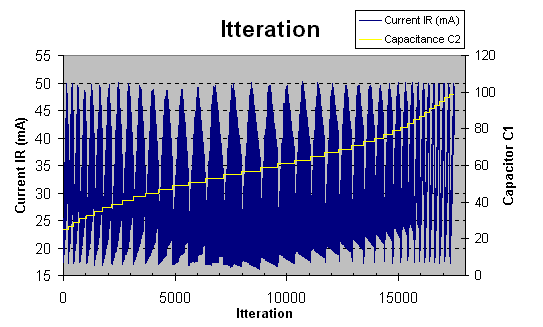
In this graph I have set the C1 to 55pF and then I calculate the current Ib at the left Y-axle for different values of capacitor C2 at the right y-axle and L. As before I save only thoose values which will give 40-60 ohm impedance. C2 is stepped from 1pF to 100pF exacltly as I did with C1 earlier. The blue curve will now show the current. As you might remember, I want the current to be as high as possible. You can see in the graph that we have several peaks all up to 50mA. When I study the values of the inductance In the data table for the graph I found that 120nH was a value which gave many high peaks. So I desided to lock the inductance to 120nH. Now, we have only C2 to play with. (se graph below)
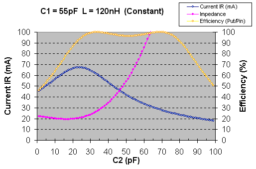
In this graph I have locked C1 to 55pF and L to 120nH. C2 will be itterated from 1pF to 100pF and I will show you the impedance and the current and finally how much of the input power that will be transformed into the base of the transistor (R).
Impedance: the pink curve show the input impedance when C2 is itterated from 1pF to 100pF. The impedance goes from 20 ohm upp to some hundred ohm. When C2 is about 47pF we will have 50 ohm input.
Current: the blue line show the current Ib into the base of the transistor (R).
Efficiency: To see how much energy that transfer into the transistor I calculated the efficiency of the matching system yellow curve. Earlier I told you that I set the Uin to 1V and I know the input impedance , I can then calculate the input energy it will consume. From my calculation I can get the current through the base Ib and I know it is 10 ohm, so I can calculate the energy into the base of the transistor. If I compare thoose two curves I will get the transfer efficiency! As you can see it will be almost 100% with the right combination of components.
We have now found the values of the three components which will transform a 50 ohm impedance to 10 ohm in the transistor with almost 100% energy efficiency. If you want to see another simulation with C1=39pF and L = 136nH click here. It might be a stoneage way to solve the calculation, but it works and it is understandable.
Puhh, That was all about the input matching. Lets have another coffee break now before we go into the last section.
Output filter (impedance transforming)
Some power formula and RMS explanation:
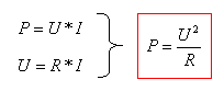 The pic at right show ohms law. As you can see from the pic I have combined the formulas and got an expresion of the power.
The formula is based on absolut values which means that the U is constant like in a DC circuit.
The pic at right show ohms law. As you can see from the pic I have combined the formulas and got an expresion of the power.
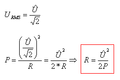
The formula is based on absolut values which means that the U is constant like in a DC circuit.This formula works well in an AC ciruit also, but we have to define the voltage by its RMS value.
RMS value depends on the shape of the signal. RMS is a factor which will be multiplied with the AC signal to generate the same effect as in a DC circuit with the same amplitude.
For example:
If we apply 12V DC over a resistor of 15 ohm, the voltage will be constant and the power will be 122/15 = 9.6W
The RMS factor for DC is = 1 (it is never printed)
The RMS factor for sine-wave AC is = 1/sqrt(2)
If I put the RMS factor into the power calculation I will get the power formula for a sine-wave AC signal.(Se fig at right)
Example:
If we apply a sine-wave AC with the amplitude of 17V to the 15 ohm we had in the DC example above we will get: 172/(2*15) = 9.6W
Conclusion: It took 12DC to get 9.6W out of the resistor but it took 17V amplitud to get the same 9.6W out from a sine-wave AC signal.
Calculating the impedance:
What we wanted to calculate from the begining was not the power, it was the impedance for the output.
We have the power formula for a sine-wave AC signal, so if we run our power amplifier with 12V DC and we want 1.44W output power, we can calculate the impedance of the output filter: 122/(2*1) = 50 ohm.
To get 1.44W output power, the transistor should see the output filter as 50 ohm.
I will explain with an example. In this PA the colector should see 50 ohm.
L, C1 C2 and R (antenna) will form the output filter. In the figure below I calculate the impedance of the filter.
When I have the expression Zin I will itterate C1, C2 and L to investigate the filter.
In the diagram below I itterate C1, C2 and L.
The blue curve shows the impedance and the yellow show the inductance. I do not display C1 and C2.
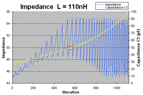
So what is interesting to see in this diagram? Well, we wanted the impedance to be close to 50 ohm and you can see, if the inductance is about 110nH you will have most chance to get 50 ohm.
I will mow lock L to 110nH and look futher into C1 and C2.
In this diagram I have locked L to 110nH and itterating C1 and C2. The blue curve is the impedance and the yellow curve shows the value of C1 and the interesting part is to see how wide the step is of the yellow curve. The wider the step is the more calculations (combinations with C2) ends up around 50 ohm.
The red ring show you the value when C1 is 49pF. At 49pF of C1 the step is wide and you have a nice impedance curve also.
I will now also lock C1 to 49pF and look futgher to C2.
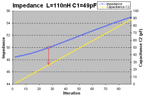
Here I have locked L to 110nH and C1 to 49pF. C1 is itterated from 1pF to 100pF. The blue curve show you the impedance and I have marked the 50 ohm impedance with a red circle. This will occure when C2 is 27 pF.
Final word
There is many different way to construct a power amplifier and there is different way to build matching networks. In this project I have tried to explain the basic function of a Class C power amplifier stage. I have simplified the construction in my explanations above and I haven't consider stray capacitans and stray inductance, still I hope I have given you some new ideas and knowledge about the subject.
You can always mail me if there is anything unclear or if you have knowledge which should be added to this page.
I wish you good luck with your projects and thanks for visit my page.