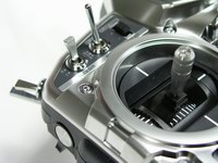
RC Receiver for airplane
This project will explain how you can build a receiver for 35MHz.
The receiver is based on the FM receiver circuit MC3371,
and the frequency is PLL controlled with LMX2306 circuit.
This project is much easier than it first may sound.
I am sure you will learn something by reading about my experimets.
All contribution to this page are most welcome!

Background
Another interst I have is radio controlling units for model airplanes.
I like the feeling of controlling a unit from distance, which is needed to fly a modell airplane.
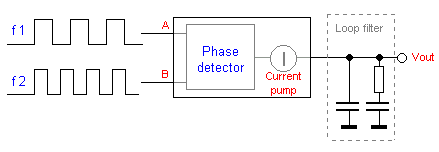
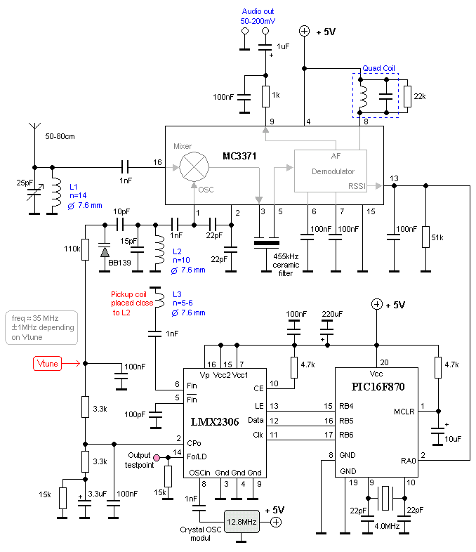
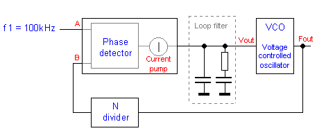
The ultimate radio controlled units are the robots sent to mars.
We actually controls a robot at another planet, isn't that cool!
Well, this project does not include rockets and mars landings…*smiling*

In this project I will build a radio receiver for RC air planes. There are 20 different frequencies (channels) used for radio controlling RC air planes. Each user needs it own frequency, else you will controll someone else plane.

The lowest frequency is 35.010MHz and the highest is 35.200MHz. In practice there are 20 different crystalls for each channel. In my receiver I have no crystal for each frequency, instead I use a frequency synthesizer. With this system I can in a very simple way choose any channel I want to receive. I will explain how a frequency synthesizer works and how you can control it.

First some words about synthesiser and PLL
(Synthesizer and PLL can be broke down into complex regulating system with lot of math. I hope all PLL experts have indulgence with my simplyfied explanation below. I try to write so even fresh born homebrewers can follow me.)

So what is a frequency synthesizer, and how does it work?
Look at the picture below and let me explain.


The hart of the synthesizer is something called phase detector, so let's first investigate what it does.
The picture above shows you the phase detector. It has two inputs A ,B and one output. The output of the phase detector is a current pump. The current pump has three states. One is to deliver a costant current and the other is to sink a constant current. The third state is a 3-state. You can see the current pump as a current delivery of positive and negative current.

The phase detector compares the two input frequencies f1 and f2 and you have 3 different states:
  • If the two input has exact the same phase (frequency) the phase detector will not activate the current pump,
    so no current will flow (3-state).
  • If the phase difference is positive (f1 is higher frequency than f2) the phase detector will activate the current pump
    and it will deliver current (positive current) to the loop filter.
  • If the phase difference is negative (f1 is lower frequency than f2) the phase detector will activate the current pump
    and it will sink current (negativ current) to the loop filter.

  • As you understand, the voltage over the loop filter will vary depentent of the current to it.

    Okay, lets go futher and make a Phase loocked loop (PLL) system.


    I have added a few parts to the system. A voltage controlled oscillator (VCO) and a frequency divider (N divider) where the divider rate can be set to any number. Let's explain the system with an example:

    As you can see we feed the A input of the phase detector with a reference frequency of 100kHz.
    In this example the VCO has this data.
    Vout = 0V give 80MHz out of the oscillator
    Vout = 5V give 100MHz out of the oscillator.
    The N divider is set to divid with 900.

    First the Vout is 0V and the VCO will oscillate at about 80 MHz. The frequency from the VCO is divided with 900 (N divider) and the output will be about 88.9KHz. This frequency is feeded to the input B of the phase detector. The phase detector compares the two input frequencies and since A is higher than B, the current pump will deliver current to the output loop filter. The delivered current enters the loop filter and is transformed into a voltage Vout. Since the Vout start to rise, the VCO frequency also increases.

    When Vout is 2.5V the VCO frequency is 90 MHz. The divider divides it with 900 and the output will be = 100KHz. Now both A and B of the phase comparator is 100kHz and the current pump stops to deliver current and the VCO stay at 90MHz.

    What happends if the Vout is 5V?
    At 5V the VCO frequency is 100MHz and after the divider (900) the frequency will be about 111kHz. Now B input of the phase detector has higher frequency than A and the current pump starts to zink current from the loop filter and thereby the voltage Vout will drop.
    The reslut of the PLL system is that the phase detector locks the VCO frequency to desired frequency by using a phase comparator.
    By changing the value of the N divider, you can lock the VCO to any frequency from 80 to 100 MHz in step of 100kHz.
    I hope this example gives you understanding of the PLL system.
    In frequency synthesiser circuits as LMX2306 you can program both the N divider and the reference frequency to many combinations.
    The circuit also has sensitive high frequency input for probing the VCO to the N divider.
    For more info I suggest you download the datasheet of the circuit.

    Click on the pic to enlarg! Schematic
    The receiver is built around the circuit MC3371 FM receiver. The oscillator is located at pin 1 and 2.
    L2 with the 15pF makes an oscillating unit. To vary the frequency a varicap is added bb139.
    By changing the voltage over this varicap the capacitance will change and the oscillating frequency will also change. The oscillator is made to work as "Voltage Contolled Oscillator" VCO.

    To control the frequency a synthesizer circuit LMX 2306 has been added. The PLL circuit has a pickup coil to pin 6. This coil should be put close to the L2 coil for picking up some of the oscillating energy. The PLL circuit has an external reference crystal of 12.8 MHz.

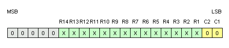
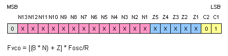
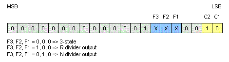
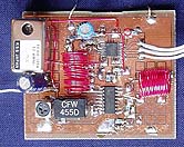
    At pin 2 of MX2306 you will find a PLL filter to form the Vout which is the regulating voltage of the VCO. The PLL try to regulate the Vout so the oscillator keeps the frequency loocked to desired frequency. The desired frequency is programmed into the PIC EEPROM and is clocked into the synthesizer (LMX2306) at power up. I will below explain how to program the EEPROM for different frequencies.
    At pin14 of the synthesizer you have a controll output. At this output you will find the reference frequency for testing. (I must warn you because the signal is not symetrical in shape. The positiv puls are only a few microsecond so you will have difficult to see it at oscilloscope.) I solved it by connecting it to a 74HC4020 14-stage Binary Counter to pin 10 Clock input. At Q0 (pin 9) you will have a symetrical square wave with half frequency since the circuit is a counter. At Q1 pin 7 it will be divided by 4, see datasheets for more info.

    Testing
    The first thing you should test is that the oscillator is working. I disconnected the Vout from pin 2 of the PLL LMX2306. I then connected Vout to ground and check the oscillator. The oscillator should now oscillate at the lowest frequency. With my "Wireless frequency counter" I found that the oscillator was working at 33MHz. I streatched the coil L2 a bit until it oscillated at 35MHz.
    I then connected Vout to +5V and now the oscillator was oscillating at 36MHz.
    Great, as "Basil" would have said!
    By changing the Vout from 0 to +5V I could change the oscillating frequency from 35 to 36MHz.
    I then reconnected the Vtune to the PLL.

    In my test I had programmed the PIC to set the frequency at 35.565 MHz = Channel 71.
    When I tested the unit again the PLL tried to regulate the Vout voltage untill the oscillator locked to 35.565MHz. I probed Vout with a DC meter and it stoped ad 0.8V and the frequency of the oscillator was now locked to the 35.565MHz. Great, great...

    How to program LMX2306
    The LMX2306 has 3 internal regist that must be set to make it work. All transfer are 21-bit long.
    The simplified block diagram below shows the R Counter, N Counter, and a Function Register.
    The data stream is shifted (on the rising edge of LE) into the DATA input, MSB first.
    The last two bits (yellow box) are the register selection control bits.

    Below you will find the reference divider. This register is selected when the C2 and C1 are 0, 0. (yellow boxes)
    By putting a divider value into the green area you will set the reference frequency.
    Example: You have a reference crystal of 12.8MHz.
    If you set the R-register (green) to divide with 1000 equal to 03e8 hex, the reference frequency will be 12.8e6 / 1000 = 12800 Hz.

    14-BIT PROGRAMMABLE REFERENCE DIVIDER RATIO (R COUNTER)


    Below you will find the divider register. This register is selected when the C2 and C1 are 0, 1. (yellow boxes)
    This register contains two parts. N part (red) and Z part (blue).
    The formula below the figure shows you how to calculate the VCO frequency.
    I think an example will help you understand.
    Let's say we want the VCO frequency to be 35.008MHz.
    Earlier we set the Reference frequency to 12800Hz, which is the Fosc/R part
    So we need to find out N part and Z part.
    If i divid 35.008e6 / 12800 I get 2735. So, 8*N + Z should be 2735. This gives me that N = 341 and Z = 7
    One important thing about Z register is that 0 =< Z <= 7
    Let's see if we got it right:
    Fvco = [(8*341)+7] * 12800 gives 35.008MHz, Great!

    PROGRAMMABLE DIVIDER (N COUNTER)


    Below you will find the function register. This register is selected when the C2 and C1 are 1, 0. (Yellow boxes)
    In the function register you can set many parameters, but I will only show you how to set it make the circuit work in a simple way.
    Three bits F3-F1 (blue boxes) set the output test pin Fo/LD.

    FUNCTION REGISTER


    Final word
    With this project I have showed you how to build a complex FM receiver for 35MHz.
    This receiver was built around synthesizer and PLL, which gives more software controlling of the receiving freqyency than the standard crystal receivers.

    You can always mail me if there is anything unclear.
    I wish you good luck with your projects and thanks for visit my page.


    Back to main Page  |  Contact Me  |  Cheap components

    Copyright © Last modified on 1 June 2004.