 1.3W Power Amplifier (Part III)
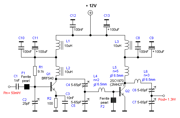 In all RF system and specially in RF amplifiers, it is very important to have a stable power supply and making sure you won't get any RF out on the power line.
The Capacitor C12 and C13 will stabilise the DC power supply.
L1, C10, C11 and L3 with C8, C9 will also prevent RF from leaking out to the powerline and
cause oscillation or disturbances. L1 and L3 should be ferrite chokes or inductance's about
1 to 10 uH.
In all RF system and specially in RF amplifiers, it is very important to have a stable power supply and making sure you won't get any RF out on the power line.
The Capacitor C12 and C13 will stabilise the DC power supply.
L1, C10, C11 and L3 with C8, C9 will also prevent RF from leaking out to the powerline and
cause oscillation or disturbances. L1 and L3 should be ferrite chokes or inductance's about
1 to 10 uH. 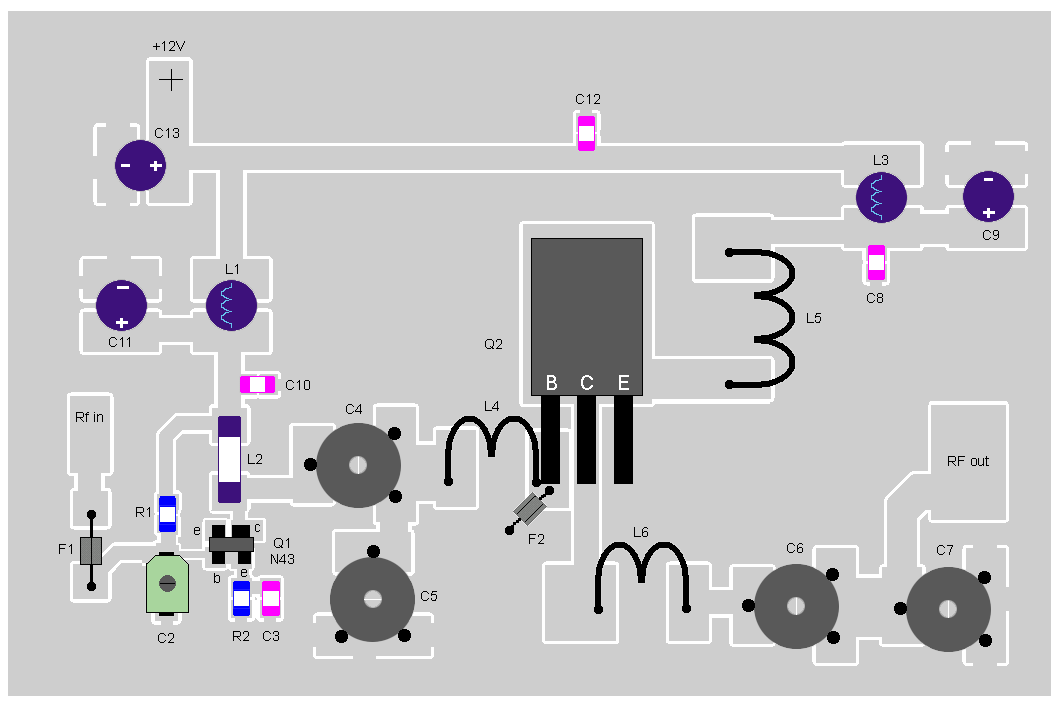
| 1wp_filled_2.pdf | PCB file for 1.3W Power Amplifier (pdf). |
 Component support