250 MHz RF generator 
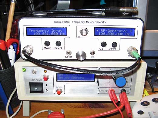
250MHz RF Generator with 1kHz display resolution
This project shows how you can build a RF signal generator with a frequency range of 0 to 250MHz.
Perfect to use for testing and tuning any radio equipment or filter.
The frequency is PLL controlled and a 2 line display shows the exact frequency.
The output frequency is a combination of digital step-tuning (50kHz),
and analogue fine-tuning (10 turn pot) to a precision of a few Hz.
This results in a very stable frequency and with a very high resolution.
You can also FM modulate the RF signal output.
All contribution to this page are most welcome!

Background
A good tool to have in the workshop is a RF signal generator.
All receiver and preamplifier need to be tuned in one way or the other.
The easiest way to tune your equipment is to inject a RF signal into the unit and tune for best signal. With a good RF generator you can also simulate IF signal (455kHz) and (10.7MHz) and test the IF part of the receiver or filters.
What is important with a RF generator?
We want it to be stable in frequency, wide frequency range, high resolution and easy to use and build.
All this has been taken in consideration while constructing this project.

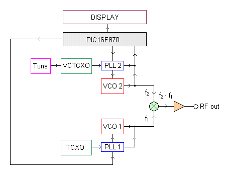
So how does it work?
Here is the basic principal of the project. (Take a look at the block diagram to the right.)
It is impossible to build an oscillator that will work from 0 Hz to 250MHz in one sweep.
The solution must be to use two oscillators (red boxes) and a mixer (green circle).
If you mix two frequencies you will get a lot of products. f1,f2, f2-f1, f2+f1 and lot of multiplier of these. The interesting product in this case is the f2-f1 product.

f1 and f2 are produced by two 900MHz VCOs which are controlled by 2 PLL circuits.
f1 will be constant at 820 MHz and f2 will step from 820 MHz to 1070 MHz.
Since the output from the mixer will be f2 - f1, we get 1070 - 820 = 250 MHz as max difference..Great! How about the other frequencies?
Well, since they all will be quit high we can use a low pass filter to reject them.

As you know, a PLL regulating system need a reference frequency to be stable and work properly.
In this project I use a very stable and exact 12.8MHz TCXO to control PLL 1 and VCO 1. This TCXO will also feed the PIC16F870.
PLL 2 and VCO 2 has a different reference frequency feed from a VCXO (Voltage controlled Crystal oscillator).
This oscillator is also very stable but the nice thing is that the frequency can be varied by a controlling voltage (Tune).

What is the purpose of that?
Well, the PLL will be able to step in 50 kHz steps, very exact and stable, and with the Tune voltage we can tune the frequency within the 50 kHz steps.
In this way you will have a digitally PLL controlled RF generator with analogue tuning possibility!!!

So how do I keep track of the output frequency?
The PIC16F870 will control both PLL 1, PLL 2 and also measure the TRUE output frequency and display it on the LCD.
In this way you will always see the exact frequency even if you are changing the output frequency by changing the Tune voltage.
  • The output frequency will be set with two switches (Inc/Dec).
  • The Tune voltage comes from a ten turn potentiometer.


  • Click here to view a larger schematic 
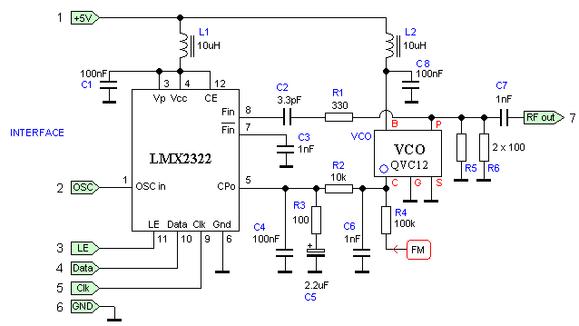
PLL controlled VCO units (800-1050MHz)
    In the block diagram above you can see that the two VCO:s and PLL have basically the same configuration.
    To make my main PCB easier to build, I decided to make the VCO and PLL units on separate PCBs.
    I can also use the VCO+ PLL in other projects in the future. Take a look at the schematic at right and I will explain.
    This little PCB contain a VCO, PLL and the component around it to make a fully functional unit. In the schematic you find the PLL LMX2322 and the VCO unit. L1 and L2 is to prevent RF on powerline. Any inductor or ferrite bead will do the job.
    Pin 5 of the PLL is the output current pump which produce a tuning voltage to the VCO.
    At pin "C" of the VCO you find the tuning voltage that set the output frequency of the VCO. Pin "P" is the output and you will have about 10mW here. Resistor R5, R6 makes a 50 ohm load which the VCO expects. You could remove the resistor R5, R6 and connect an antenna here and have a PLL controlled transmitter working from 800-1050MHz. There is a frequency feedback to the PLL by R1 and C2 which the PLL. I have not implemented any reference oscillator on this pcb because I want a general solution which can be used in all kins of other constructions. You can FM modulate the RF signal of the VCO, by applying your signal to the input labelled FM in a red box.

    Click here to view a larger photo 
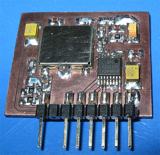
This PLL controlled VCO unit has 7 connection (green).
  • + 5V input
  • Reference oscillator input
  • LE input
  • Data input
  • Clock input
  • Ground input

  • Power output


  • Some measurement of output frequency with input voltage pin C of VCO
    0.1V => 815 MHz
    0.8V => 850 MHz
    1.8V => 900 MHz
    2.8V => 950 MHz
    3.8V => 1000 MHz
    4.8V => 1050 MHz


    Click on the pic to see a larger format. 
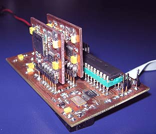
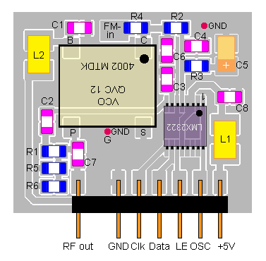
PCB of the PLL controlled VCO units
    inject.pdf PLL controlled VCO units (pdf).

    Above you can download a (pdf) filer which is the black PCB.
    The PCB is mirrored because the printed side should be faced down the board during UV exposure.
    To the right you will find a pic showing the assembly of all components on the same board.
    This is how the real board should look when you are going to solder the components.
    It is a board made for surface mounted components, so the copper is on the top layer.

    Grey area is coppar and each component is draw in different colours all to make it easy to identify for you.
    The scale of the pdf is 1:1 and the picture at right is magnified with 4 times.
    All component for PLL controlled VCO units (Click here to download component injct.txt).

    Click here to view a larger schematic 
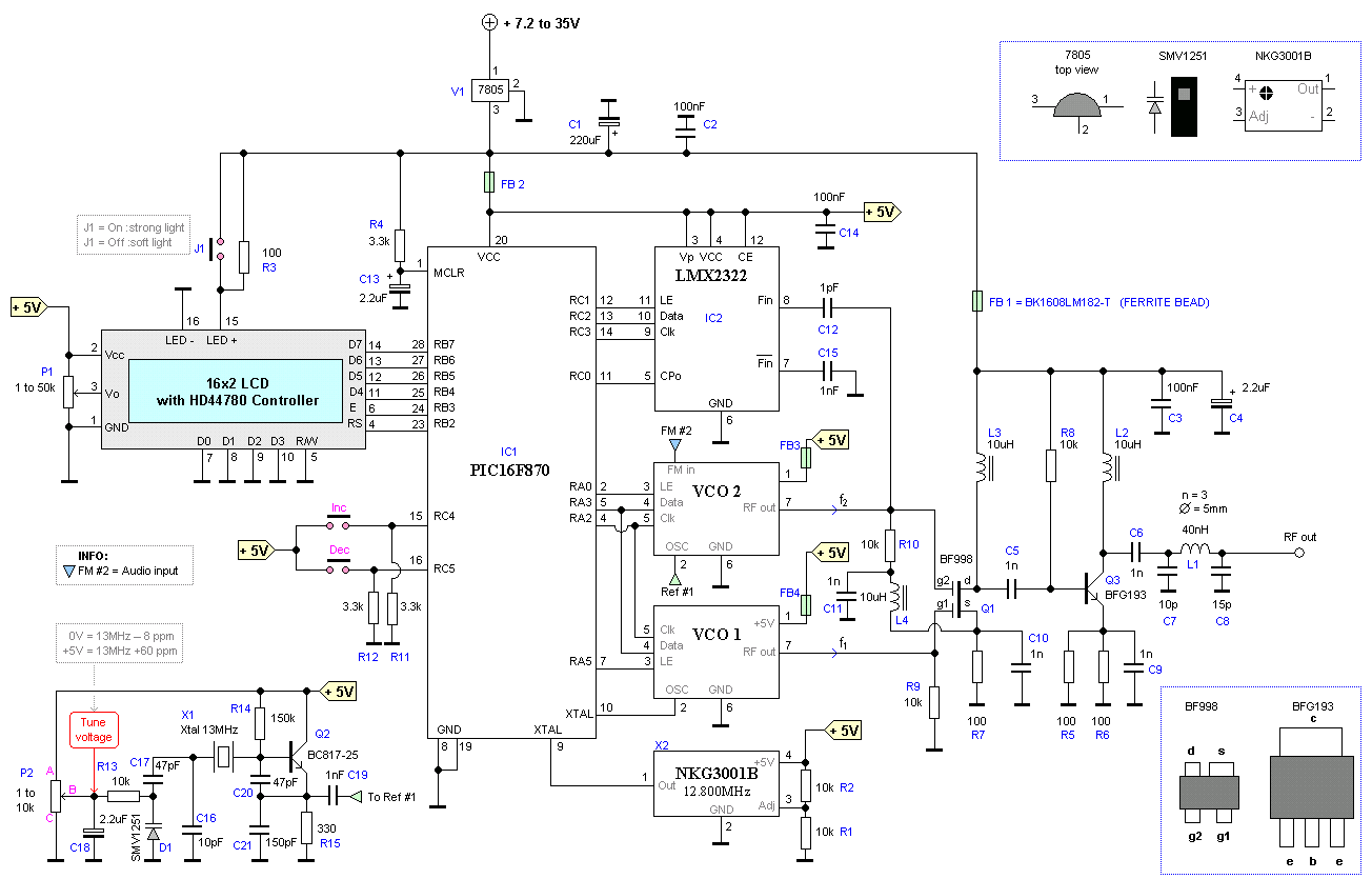
RF generator hardware and schematic
    Click on the right picture to see the main schematic of the unit. Let's identify the different blocks.
    To the left you will find a 2 line x 16 Char LCD display.
    It use a HD44780 controller which is very common. J1 is a jumper which will give the LCD a strong or soft back light.
    In the middle you will find the PIC16F870 which will handle all controlling.
    To the left you will find the two VCO modules labelled VCO2 and VCO1.
    Take a look at VCO1. The reference frequency for this VCO is set by a 12.8MHz module (NKG3001B).
    The frequency is very exact and as you see it also drive the PIC16F870. The output frequency from the VCO1 (pin 7) is feed to gate 1 of a dualgate FET which will act as a mixer. The RF output (pin 7) of the VCO2 is connected to gate 2 of same dualgate FET.
    The gate 2 of the dual gate FET is DC biased and the FET will work in a non linear way to produce a mixing product of the two frequencies f2 and f1.
    The output product frequency (f2-f1) will be amplified in the BFG193 transistor and a low pass filter cleans up the output RF signal from unwanted frequencies.
    The frequency from the VCO2 is probed by a LMX2322, which will measure the output frequency and make the PIC16F870 display the exact output frequency from the mixer. The reference frequency (Ref#1 on schematic) to VCO2 is connected to (pin 2) and comes from our voltage controlled crystal oscillator which you will find at the left bottom corner.

    Here you will see a crystal oscillator based around a 13MHz crystal. To make it voltage controlled, I have added a varicap diode which will make it possible to adjust the frequency (-8 ppm to + 60ppm) by changing the Tune voltage from 0V to + 5V.
    The Tune voltage comes from a potentiometer. If you want really fine tuning you can use a 10 turns potentiometer.
    Since we can adjust the reference frequency to VCO1, the output RF frequency from VCO1 will also be changed.
    So if you change the reference with 1ppm you will change the output frequency 1ppm.
    Example:
    -8ppm = -8e^6 *1000 = -8kHz at 1000MHz.
    +60ppm = 60e^6 *1000= 60kHz at 1000MHz.
    This means that VCO2 can be changed about 68kHz in an analogue way by a potentiometer. The digital step will change the RF from 820 to 1070 MHz.
    In this great way you can get advantage from both a digital and analogue system to generate a RF signal from 0 to 250MHz.

    If you wish to FM modulate the RF signal with an audio or digital signal, you can connect the signal to the ( FM #2 ) input of the VCO2.
    Any AC signal connected to this input will directly modulate the RF output signal. It can be very good option to use for testing your receiver.

    All system in this unit use +5V which comes from V1 (7805) circuit.
    A jumper J1 is added to choose if you want strong backlight or not.
    If jumper J1 is disconnected the LCD will have soft backlight because a low current will pass through R3.
    If jumper J1 is connected you will have strong backlight.
    More details will be found under assembly and testing.

    Click on the pic to see a larger format. 
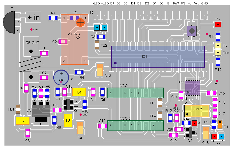
Main PCB of the RF generator
    rfg.pdf Main PCB of RF generator (pdf).

    Above you can download a (pdf) filer which is the black PCB.
    The PCB is mirrored because the printed side should be faced down the board during UV exposure.
    To the right you will find a pic showing the assembly of all components on the same board.
    This is how the real board should look when you are going to solder the components.
    It is a board made for surface mounted components, so the copper is on the top layer.

    Grey area is coppar and each component is draw in different colours all to make it easy to identify for you.
    The scale of the pdf is 1:1 and the picture at right is magnified with 4 times.
    All component for Main PCB RF generator (Click here to download component injct2.txt).

    The scale of the pdf is 1:1 and the picture at right is magnified with 4 times.

    Assembly
    Good grounding is very important in a RF system. I use bottom layer as Ground and I connect it with the top layer at six places (via-holes) to get a good grounding.
    Drill a small hole through the PCB and solder a wire in each via-hole to connect the top layer with the bottom layer which is the ground layer. The six via-holes can easy be found on the PCB and in the assembly pic at right, they are labelled "GND" and marked with red colour. Drill the remaining 16 holes for the pin header 2.54mm which will connect the LCD to the PCB.
    Since the backplane of the PCB is Ground you must make sure there is no connecting copper to the pin header 2.54mm at the backside. Easiest way is to remove the coppar at the backside is to use a larger drill (3mm) and drill a bit in the holes at the backside of the PCB.

    The first assembly step is to connect the PIC and make sure the LCD starts up.
    So, connect these parts:
    V1, IC1, X1, X2, J1, Display, INC and DEC buttons, Q2, D1
    C1, C2, C13, C14, C16, C17, C18, C19, C20, C21
    R1, R2, R3, R4, R11, R12, R13, R14, R15, P1, P2
    FB1, FB2, FB3, FB4

    When power is applied, the LCD should wake up and display information text.
    P1 should be set so the voltage at pin 3 of the LCD should be about 0.70V to 0.75V. This will give good contrast!
    You can now also make sure that the frequency from the 13MHz oscillator (Ref #2) is working.

    Since we have not connected any VCO:s and IC2, the display will not show correct frequency.
    When we knows that the PIC is running and the display is working we can go further to test the VCO:s. Connect the VCO 1/VCO 2.
    A good thing is to test them separately.
    If you push both INC and DEC buttons at same time the PIC will go into a "SILENT MODE" then it will go into "VCO TEST MODE"
    In the VCO test mode the PIC will set each VCO to 820/850/950/1000MHz.
    The software keeps changing the VCO every 5 seconds and starts over until you push any buttons again.

    This mode will help you to test the function of the VCO:s. You can either use a frequency counter to verify the VCO or you can measure the tuning voltage pin C of the VCO. You can read more in PIC software section below.
    When both VCO:s are working you can add the rest of the components. When all components are attached, you should see the output frequency on the display.
    If you still wont see any frequency on the display, I advice you to check the soldering of the IC2. Make sure you have no soldering bridges.

    Soldering the hole mounted components
    X2 can be a little bit tricky to solder since its legs are a bit short. Before you solder X2, make sure you have solder C2 and R2
    Connect the LCD to the PCB with the (Pin Header 2.54mm). The LCD is placed at the back side of the PCB.
    In the photo at top of the page, I have used a flat cable to connect the LCD.
    You can also see the two VCO:s standing up. In my test unit I use a socket (green) for the PIC16F870 because I needed to test and reprogram it.

    The desoldering wick is a flattened, braided copper sheath	Soldering the surface mounted components
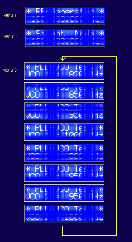
    Here comes the big challenge. Click here to see photo and read how to solder SOIC and smd components.
    The LMX2322 circuit is a fine pitch SO-IC circuit and this little bug can make your life miserable.
    Don't worry I will explain how to handle it. Use thin lead solder and a clean soldering tool.
    I start by fixate one leg on each side of the circuit and makes sure it is correct placed.
    Then I solder all other legs and I don't care if there will be any lead bridges.
    After that it is time to clean up and for that I use a "wick".
    The desoldering wick is a flattened, braided copper sheath looking for all the world like shielding on phono cord (except that the shielding is tinned) without the cord.
    I impregnate the wick with some rosin and place it over the legs and bridges of the circuit. The wick is then heated by the soldering iron, and the molten solder flows up the braid by capillary action.
    After that, all bridges will be gone and the circuit looks perfect.
    You can find wick and rosin at my component page.

    PIC Software
    Let's have a look of the different menu systems and choices of this frequency generator. All settings are made by the two switches INC and DEC.
    Figure below show all the different menu choices.

    When you start the unit, the display will show you the output frequency (MENU 1).
  • By pressing INC button the unit will step up 50 kHz. If you hold the button pressed the unit will continue to increase the frequency with larger steps.
  • By pressing DEC button the unit will step down 50 kHz. If you hold the button pressed the unit will continue to increase the frequency with larger steps.

  • By holding the button pressed, you can easy INC or DEC the hole frequency range within a few seconds.
    The display present the frequency 2-3 times/ second and the resolution is 1kHz.

    Since there is lot of data transmission to the LCD you might get "digital glitches" and disturbance on the RF. It is very difficult to get rid of small digital disturbances in a RF construction. Sometime you might want to have a very clean RF signal.

  • If you press both INC and DEC at the same time you will enter MENU 2, called "Silent Mode".

  • In this mode you will have no update on the display, but the generator will still work. The RF line is now silent from all "digital glitches".
    By pressing INC or DEC, you will go back to MENU 1 again.

  • If you are in MENU 2 and you press both INC and DEC at the same time you will enter MENU 3.

  • The "MENU 3" is only for testing the VCO:s. In this Menu, the two VCO:s will be set to the frequency 820, 850, 950 and 1000 MHz. The display show what happens all the time and each frequency is set for 5 seconds. When VCO 2 has reached 1000MHz it all starts over again and VCO 1 sets to 820MHz.
    This test mode is good thing to have when you test the function of the VCO:s. You can either measure the output frequency of the VCO:s with a frequency counter or you can measure the VCO voltage from the LMX2322 circuit that control the two VCO. Look at the table above to see my measurements.

  • The RF generator will always remember the last frequency settings, even if power is switched off.


  • Download PIC16F870 programs (INHX8M format)
    Here you can download the software for this project. The zip file contains hex file made for this project.

    rf_generator_v11.zip PLL software to 250MHz RF Generator (the hex files are zipped!).

    KIT
    All parts can be found on my component page www.rfcandy.com.
    If you wish to order a KIT, please Contact Me.

    In this part, I describes a very powerful frequency counter with high sensitivity and smart software functions.
    Beside all that, it looks pretty cool.

    Building manual
    Mr Piet O and Jesse K, has sent me a very professional PDF-manual,
    where they describe how they built this frequency unit and what they bumped into during the assembly.
    Great work Piet and Jesse! We all thanks you for your effort.

    Download PDF manual
    250MHzRFgenerator.pdf (632kb)
    Click here to download file

    Final word
    A good RF generator is a tool we all need in our radio experiments.
    In this project I have tried to build a stable frequency generator and still make it simple to build.

    You can always mail me if there is anything unclear.
    I wish you good luck with your projects and thanks for visit my page.

    Photo Gallery
    Some assembled counters people has mailed me. Please mail me more.

    Piet constructions. I am impressed!    Click the pic to see larger photo!

    Back to main Page  |  Contact Me  |  Cheap components

    Copyright © Last modified on 02 Dec 2006.