We see you without your knowledge and aproval, don't ever forget that. We can also park a misil in your garage.... 
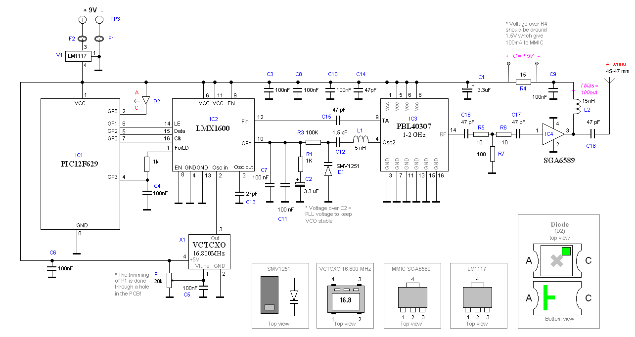
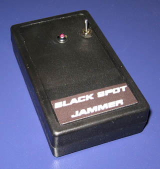
The Black Spot II - GPS Jammer with 7.2W EQP
Better performance, longer jamming range and more rf power
All knowledge can be used in a good way or a bad way.
It is up to you to use this knowledge with high moral and responsibility.

You can also call this project "PLL controlled transmitter", because it is simply a transmitter.
It is the software that define frequency and what this transmitter will do.

The transmitter works from 1 GHz to 2 GHz and the frequency is controlled by a PLL system.
For example, if you need a stable RF carrier at 23cm band, you can use this project as well.

Weather it is legal or not to use this transmitter at some frequencies, is up to you to find out.
I take no legal responsibility for any use of the product.

The construction is extremely simple and you do not need to be expert to build this.

Features:
  • Wide VCO frequency range 1000 MHz to 2000 MHz.
  • High frequency stability and accuracy ± 10 Hz
  • High output power, equivalent power = 7.2 W EQP
  • Transmitting range 500-800m (1600-2500 feet)
  • Frequency Lock Detection
  • Small size 1" X 1.8" (25 mm x 46 mm)
  • 7-15 V DC power supply, 9V battery is default
  • No complex tuning
  • Self-test with LED indication
  • Blue LED flash indication of operation.
  • Blocks all known GPS and trackers on the market today.
  • Simple to build and test.
  • Jammer with same size as a 9V PP3 battery. Transmitting distance 500-800m
  • This project comes only in a KIT version, see more details below

  • All contribution to this page are most welcome!

    Background
    If you are new here and wonder about the background and the purpose of this project,
    I advice you to visit the first project Black Spot.

    It was time to upgrade the old jammer. I have put focus on simplicity. Simplicity is the state or quality of being simple.
    It is easy to build a project and get it working, but to replicate it with same good performance is quit a trick.
    Dealing with GHz is not the most fun part in life, specially when it comes to making circuits boards.
    The journey of Black Spot II, started with some experiment of a VCO circuit called pbl40307.
    It is basically a dual VCO for mobiles, and this litter bugger showed impressive performances.
    The frequency range and the stability was very good and with few external parts.
    A new PLL circuit LMX1600 has been chosen because it is very good circuit and have a great frequency Lock Detection function.
    To keep the frequency stable I use the well known 16.8 MHz reference crystal.
    To boost the RF power I have chosen a SiGe HBT MMIC Amplifier SGA-6589 with great gain and output power.
    A microcontroller handle all communication to the PLL circuit and also control that the PLL is Locked and stable.
    More details will be explain in section hardware below.


    Hardware and schematic
    The main part of this project is a VCO based on the circuit PBL40307, a PIC12F629 and a PLL LMX1600.
    The PIC control the PLL through LE, Data and clock input and set the PLL to lock the VCO to the GPS frequency 1.57542 GHz.
    A feedback system (C15) from PBL40307 feeds the PLL with RF signal. The PLL output CPo (pin 10) will control the VCO with a tuning voltage (voltage to varicap D1).
    The tuning voltage is built up from the PLL filter C7, C11, R1 and C2. You can measure/monitor the tuning voltage over C2 or directly at pin 10 of PLL circuit.
    The VCO range is about 1530MHz to 1610MHz with applied voltage 0 to 5V.
    When locked to 1575.42MHz, the voltage should be around 2.5V, but can vary much. Anything from 1 to 4 V can occur.
    The reason of this wide range 1-4V is because of variation in the VCO range due to the parts L1, C12 and D1.
    The values of the parts are never exact, so small differences can give different VCO range. Even the soldering affect the values.
    If the voltage is 0V or +5V, something is wrong.
    Click on rhe picture to enlarge. 
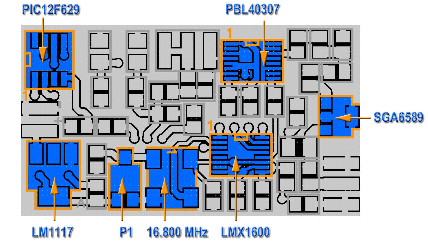
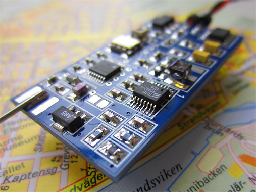
The nice thing with LMX1600 is that it has a FoLD (Lock Detect) output pin 1.
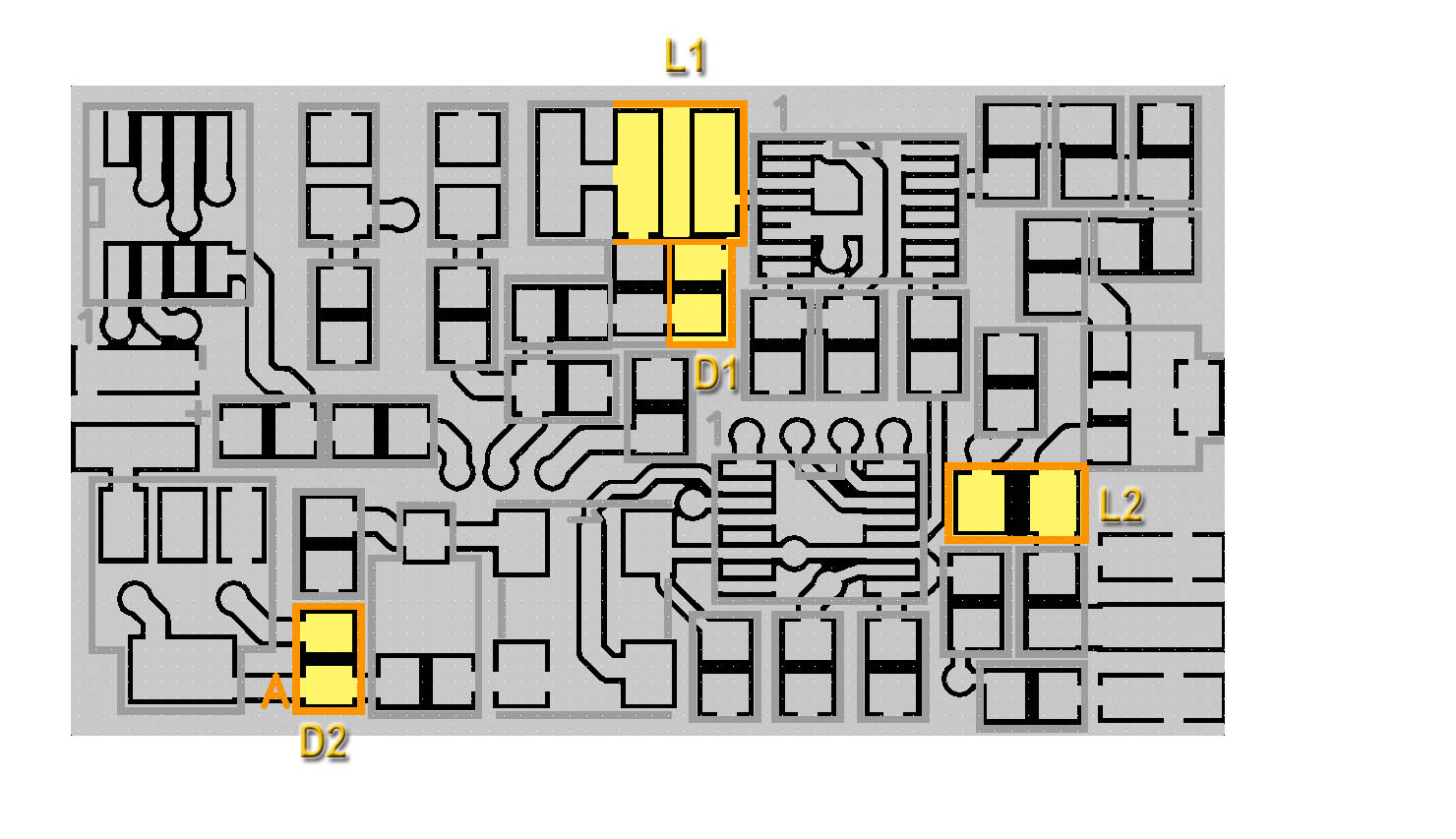
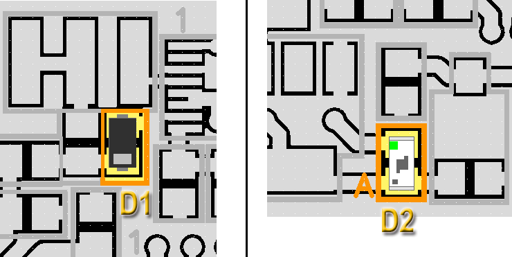
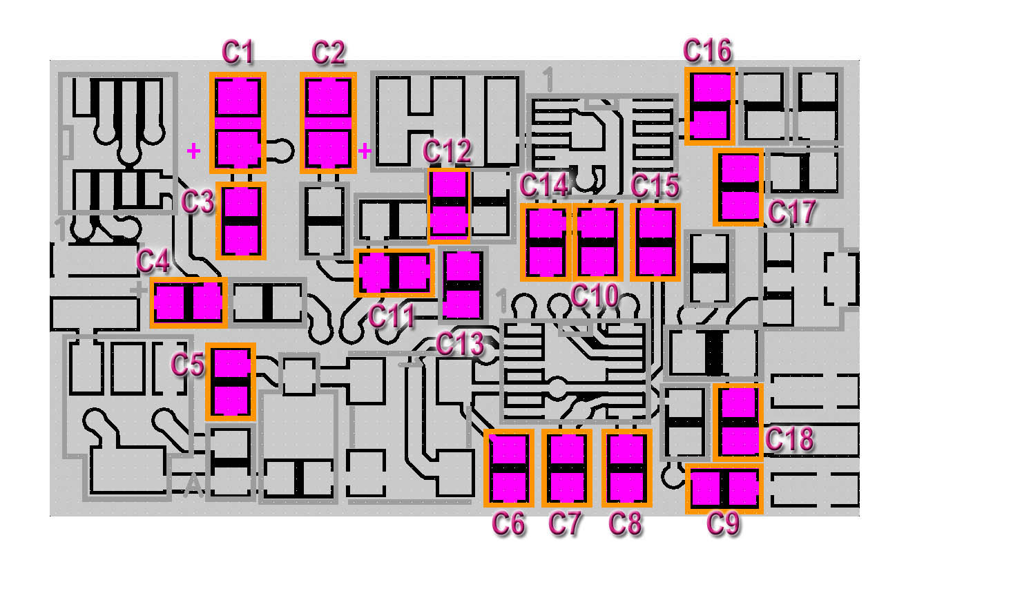
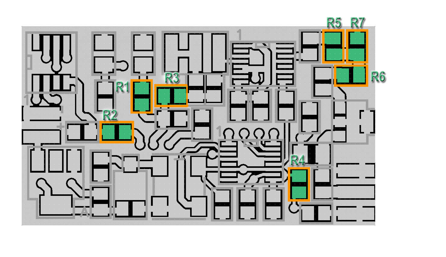
    When this output is high, the VCO is stable and locked to the desired frequency.
    X1 is a 16.800 VCTCXO oscillator which acts as reference frequency. It feed the PLL circuit to create a reference frequency for the regulating system.
    A pot P1 is added to fine tune the VCTCXO frequency. X1 is a very stable and exact oscillator.
    You will achieve best performance from the unit if X1 is calibrated with a frequency counter.
    Still, the VCTCXO is so precise that the unit will work even if X1 is not tuned perfectly.

    The output of from VCO PBL40307 is directly connected to an attenuator based of resistors to form about 5dB attenuation.
    The signal is then feed o the MMIC.
    The purpose of the attenuation is to form a good impedance system for the VCO and to prevent reflections from the MMIC.
    The output from the MMIC is feed to the antenna system. The current to the MMIC is feed from resistor R4.
    You should monitor the current though R4. Easiest way is to measure the voltage over R4 and divide it with 15.
    The voltage should be about 1.5V (see schematic) and the current should be around 90 - 100mA.
    You can lower this current by increasing the value of R4. You can also increase the current by lowering the value of R4. (R4 should be from 10 to 30 Ohm)
    Although I advice you to stay around 100 mA since you can blow the MMIC with to much current.
    The more current the higher gain and more output rf power.
    This is a typical GPS tracking on the market.
    A diode D2 is added to indicate that the PIC and the PLL is alive and kicking. The LED will blink ONE time per second to indicate jamming function.
    If the PLL doesn't lock properly due to some reason, you will get DOUBLE blink of the LED. A double blink indicate error.
    The antenna is a whip of 45 mm. The antenna gain is 0dB and it has been the reference of my measurements.
    You can of course you a better antenna with much more gain and thereby get much better performances and longer transmitting range.
    Some antenna links: Homebrew GPS antenna

    PCB and KIT
    I will not present the PCB for this project, because the system works at 1-2 GHz which require a double side factory made PCB.
    The PCB is double side and have many via holes. A factory made PCB also makes the soldering so much easier.
    If you wish to buy a complete KIT with a factory made PCB, you can go down to section named "KIT" a bit down. Click here to jump down!

    The desoldering wick is a flattened, braided copper sheath Assembly
    The soldering of this unit is pretty basic. I will explain how to assemble this KIT step by step.
    The PCB is a factory manufacture PCB with high quality, which makes the assembly and soldering simple.
    Please do not be scared for soldering smd parts. Smd is not more difficult than hole mounted parts if you use the correct skills and tools.
    Important tools are good light, soldering tool with thin tip, magnifying glasses, tweezers, thin soldering lead, wick impregnated with rosin and calm mind.

    The de-soldering wick is a flattened, braided copper sheath looking like shielding on phono cord (except that the shielding is tinned) without the cord.
    The wick is impregnated with rosin. Place the wick over the legs or bridges of the circuit.
    The wick is then heated by the soldering iron, and the molten solder flows up the braid by capillary action. After that, all bridges will be gone and the circuit looks perfect.
    Thin soldering lead and wick impregnated with rosin are included in the KIT.
    Click here to see photo and read more examples how to solder SOIC and smd components.

    There are four steps for mounting the parts. Below I describe them with picture and instructions. Some picture can be magnified by clicking onto the picture.

    Please follow the mounting instruction below
    (You can click on all pictures below for higher resolution)

    Picture below show placement of all parts.
    Click on rhe picture to enlarge.

    Picture below show placement of circuits and pot.
    Click on rhe picture to enlarge.

    Start by mounting IC1 (PIC12F629), IC4 (SGA6589 MMIC), V1 (LM1117), X1 (16.800 MHz ), P1 (Pot 20k), IC3 (PBL40307) and IC2 (LMX1600).
    IC2, and IC3 is the big challenge, but since we have a factory made PCB, thin lead and wick, you will handle it with no problems.
    The circuits are a fine pitch SO-IC circuit and those little bugs can make your life miserable.
    Don't worry I will explain how to handle it. I use very thin solder lead and I always use a soldering tool with sharp tip.
    (Thin solder lead and wick will be added in the KIT)

    I start by fixate one leg on each side of the circuit and makes sure it is correct placed.
    Use magnifying glasses to control that the leg pattern matches the PCB patterns.
    Make sure you have placed the circuits in correct directions!
    Then I solder all other legs and I don't care if there will be any lead bridges.
    I use the "wick" to clean up and to remove any bridges.

    Sometimes it is good to reheat the legs without adding any more lead.
    The circuits is now soldered and without any bridges.

  • IC1 = PIC12F629 CPU

  • IC3 = PBL40307 RF VCO

  • IC2 = LMX1600 PLL

  • IC4 = SGA6589 MMIC

  • X1 = 16.800 MHz Crystal Module

  • V1 = LM1117 Voltage Regulator

  • P1 = Pot 20k (Make sure you mount it so it can be adjusted trough the hole in the PCB)

  • Make sure that you mount all the circuits in correct orientation!
    Click here to see detailed picture

    Picture below show placement of varicap, LED and inductors.
    Click on rhe picture to enlarge.

  • D1 = SMV1251 (make sure you mount it in correct direction, see detailed picture below.)

  • D2 = LED ( D2 is a blue LED diode. This diode must be placed in correct direction.
    It has a green marking indicating cathode side and at the bottom you also find a marking.
    See detailed picture below and at the schematic.
    )

  • L1 = Inductor 5 nH

  • L2 = Inductor 15 nH

  • Click here to see detailed picture

    Picture below show detailed placement of varicap and LED.
    Click on rhe picture to enlarge.

    Picture below show placement of capacitors.
    Click on rhe picture to enlarge.

  • C1, C2 = 3.3 uF (Orange line = positive)

  • C3, C4, C5, C6, C7, C8, C9, C10, C11 = 100 nF

  • C12 = 1.5 pF

  • C13 = 27 pF

  • C14, C15, C16, C17, C18 = 47 pF

  • Click here to see detailed picture

    Picture below show placement of resistors.
    Click on rhe picture to enlarge.

  • R1, R2 = 1.0k Ohm

  • R3 = 100k Ohm

  • R4 = 15 Ohm

  • R5, R6 = 10 Ohm

  • R7 = 100 Ohm

  • Click here to see detailed picture

    Testing and tuning
    The testing of this unit is pretty simple, since it has built in test software.
    Apply power to the unit. Directly after power up the LED D2 will blink ONE time and the PLL will lock the VCO to frequency 1575.42 MHz.
    The LED will now start pulsing in intensitiy during five seconds. During this five first seconds the frequency is constant and stable.
    You can connect a frequency counter to the transmitter and check/tune the output frequency by turning pot P1.

    A simple way to measure frequency is to connect a 45 mm (1.8") wire to the input of your frequency counter. The wire will act as "pickup" antenna.
    You can now simply hold the transmitter close the "pickup" antenna and read the results from your frequency counter.

    After the five first seconds, the transmitter starts jamming and jumps around many frequencies.
    The LED will blink ONE time per second to indicate jamming function.
    If the PLL doesn't lock properly due to some reason, you will get DOUBLE blink of the LED.
    A double blink indicate PLL error.

    IMPORTANT:
    If you get double blink of the LED, the PLL does not lock properly and you have bad function.
    You will find more information in the trouble shooting section below.

    You can now control the PLL system by measure the PLL voltage over capacitor C2 or at pin 10 of the PLL. (see schematic)
    The voltage here should be a stable voltage of about 2.5V DC. The voltage can vary from VCO very much.
    If the voltage is 0V or +5V, something is wrong. (see trouble section below)

    The reference oscillator frequency can be found at pin 3 of the 16.8MHz VCTCXO. You can also find it at pin 2 of the PLL.
    Since the 16.8 MHz VCTCXO is very exact in frequency, you will get good functionality even if it is not tuned correct.
    Although, the more exact reference frequency you have, the better jamming you will get.
    The best way to tune the unit is to connect a frequency counter and tune P1 till you get 1.57542 GHz


    GPS Jammer with 7.2W EQP KIT KIT Assembled in protective box
    Black Spot jammer assembled into a protective box with with battery cover. A button for switch ON/OFF and LED indicator.
    Black Spot jammer assembled into a protective box with  button for switch ON/OFF.

    Demonstration VIDEO
    Here you can download and look at a demonstration video during a test with U-blox GPS receiver module.
    The module is connected to a computer running U-blox evaluation software. The jammer is placed 100 feet from the GPS receiver.
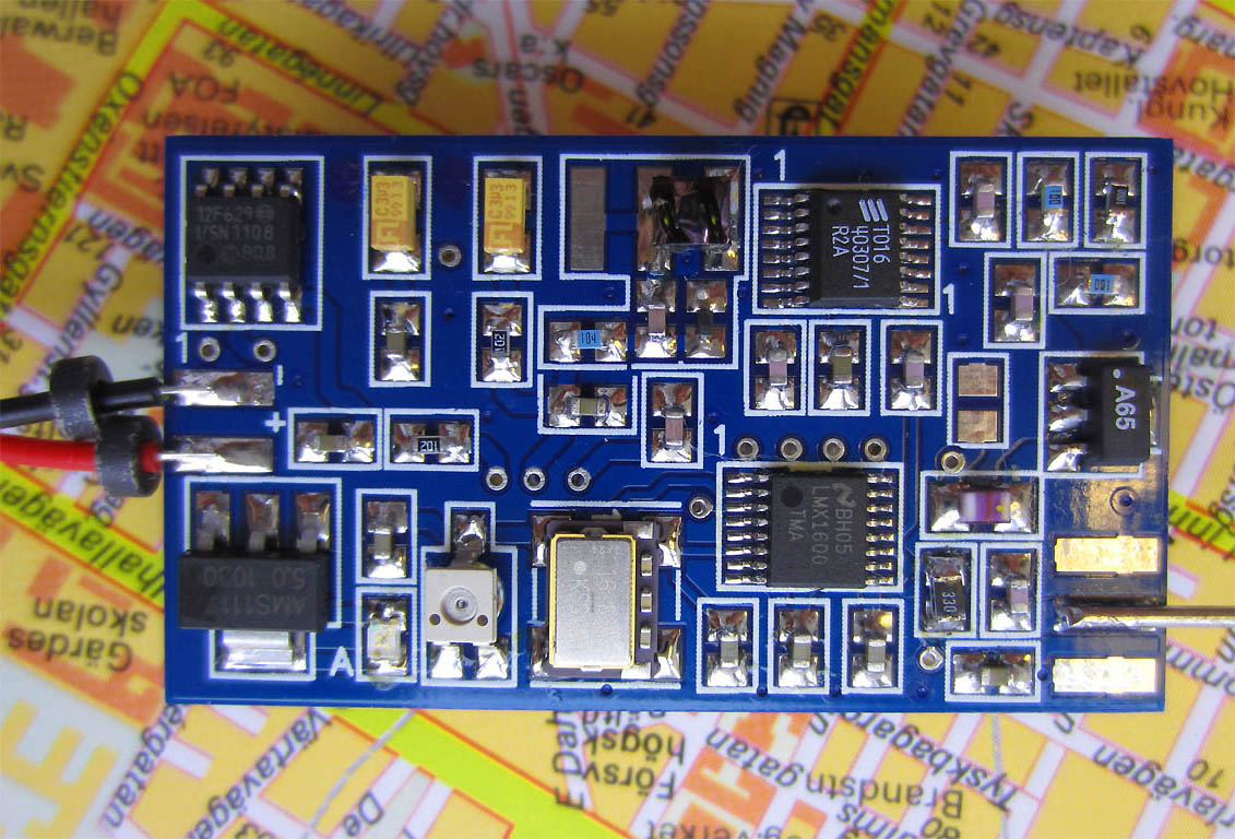
    jammer.avi
    Youtube clip of jammer.avi
    download video (4.5 Meg).

    KIT
    I have put together an educational KIT with a factory made PCB.
    You can also buy an assembled KIT which is tested, tuned and ready to use. (More info below)
    All parts needed are included in the KIT (Click here to download component list.txt).
    Order a KIT
    which will include all parts

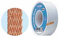
    The Blackspot II - KIT includes all parts, manual, soldering lead, and wick.

    Order here

    Click here to go to shop


    Custom made units

    If you have any special requirements when it comes to frequency, function, soldering or software, please e-mail me.


    Trouble Shooting section
    If you get a problem with your unit, you might find this section helpful.
    A general rule is to check that you have proper soldering without any bridges.

  • I get no blink from the LED diode D2!

  • Make sure you have placed the PIC in correct way.
    Make sure you have + 5V to pin 1 of the PIC12F629.
    > Check that the LED diode is placed in correct direction.
    Check with oscilloscope the you get pulse from pin 2 PIC12F629.
    I often use a small speaker or piezo element and listen to the signal.
    You should hear clicking sound or beeping tone once per second.

  • I get double blink the LED diode D2 all the time!

  • This indicates that there is a problem for the PLL to lock the frequency.
    There can be many different errors causing this.
    Make sure you have + 5V over capacitor C1.
    Make sure you have placed the IC2 and IC3 in correct direction.
    Make sure you have 16.8MHz oscillation on pin 3 of the crystal and also at pin 2 of the PIC12F629.
    The reason can be bad soldering of the L1, C12, Varicap D1.
    Make sure you have placed the varicap D1 in correct direction. (see schematic)
    You can disconnect the MMIC section by removing R4. The unit will work but with less power.
    It can be bad antenna soldering, or wrong length of antenna.
    It can also be that the antenna is touching something that creates reflections of power.
    Make sure the PLL get data, clock and CE signal.
    Check with oscilloscope the you get pulse from pin 5, 6, and 7 of PIC12F629.
    I often use a small speaker or piezo element and listen to the signal.
    You should hear clicking sound or beeping tone once per second.

  • I get 0V or +5V over capacitor C2 !

  • Your PLL system is probably not locking.
    Make sure you have placed IC2 correct and that you have proper soldering.
    Measure that you have reference frequency on pin 2 IC2.
    Check all other parts involving the PLL filter.
    If you have a frequency counter, you can connect it to VCO output or the MMIC output and
    apply a DC voltage to pin 10 of the LMX1600.
    The VCO should then change frequency when the voltage changes.

  • I have no voltage over R4!

  • This means that you have no current running through the MMIC.
    Make sure you have soldered L2 correct. If you have +5V on one side of L2 and 0V on the other the soldering is bad


    If you have any problems, you are always welcome to e-mail and I guarantee we will fix it.

    Final word
    I hope you have had a fun time assembly this KIT.
    The project may be a small one, but still it is a very powerful unit.
    Thanks for your time…

    Gallery

    Picture gallery of Trinity RF Power Meter. Click the picture to see larger views.

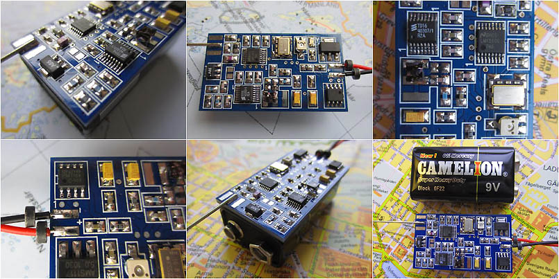
    Click the picture above to see the picture gallery.


    Back to main Page  |  Contact Me  |  Cheap components

    Copyright © Last modified on 28 Mars 2012.